Computer vision systems aren’t necessarily restricted to solely analyzing the portion of the electromagnetic spectrum that is visually perceivable by humans. Expanding the analysis range to encompass the infrared and/or ultraviolet spectrum, either broadly or selectively and either solely or in conjunction with visible spectrum analysis, can be of great benefit in a range of visual intelligence applications. Successfully implementing these capabilities in traditional PC-centric hardware and software configurations is challenging enough; doing so in an embedded vision system which has stringent size, weight, cost, power consumption and other constraints is even more difficult. Fortunately, an industry alliance is available to help product creators optimally implement such vision processing in their resource-constrained hardware and software designs.
All objects emit radiation, with the type of radiation emitted primarily dependent on a particular object’s temperature. Colder objects emit very low frequency waves (such as radio, microwaves, and infrared radiation), while warmer objects emit visible light or higher frequencies (ultraviolet, for example, or x-rays or gamma radiation). This spectral expanse is called the electromagnetic spectrum (EMS), and consists of all wavelengths from radio waves at the low-frequency end of the range to gamma rays at the high-frequency endpoint (Figure 1).
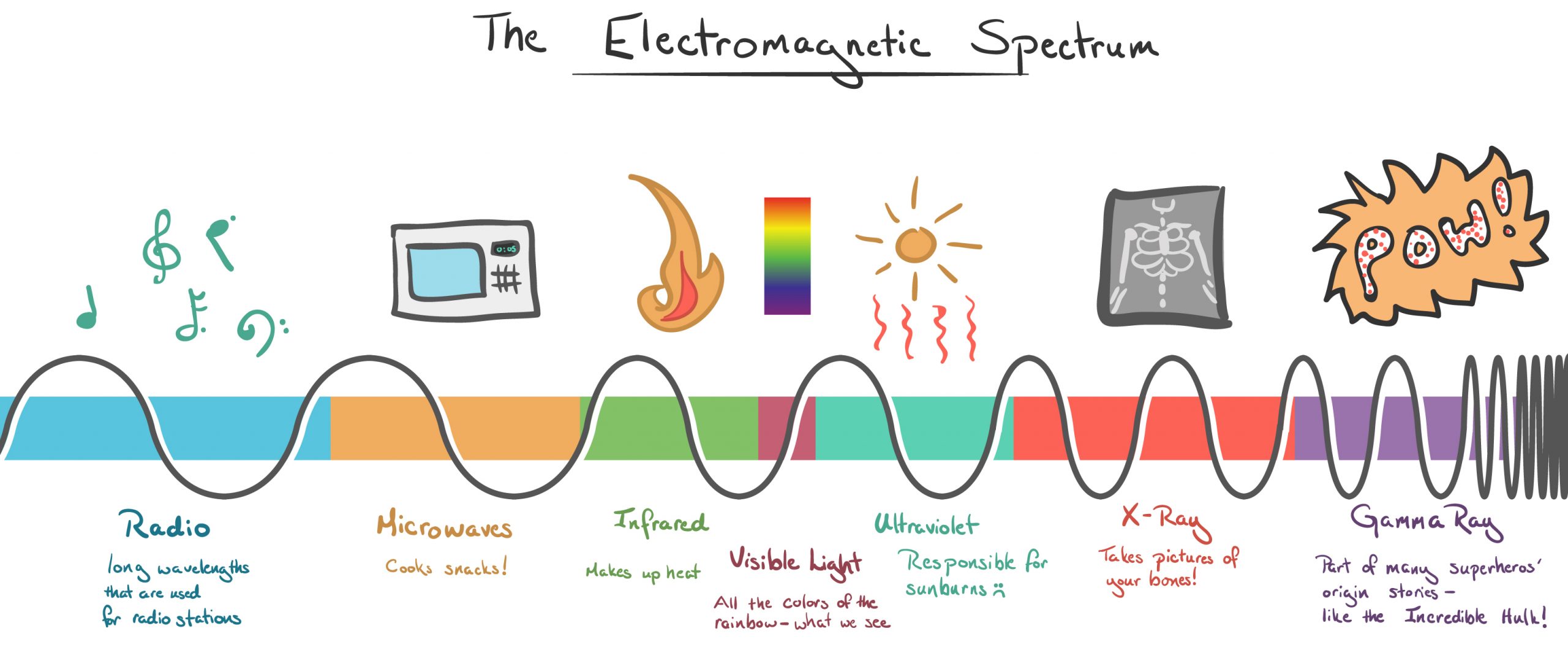
Figure 1. The electromagnetic spectrum encompasses wavelengths from radio waves to gamma rays, both selectively emitted and absorbed by various objects (courtesy Khan Academy).
Just as different objects emit radiation at different frequencies, different materials also absorb energy at different wavelengths across the EMS. A radio antenna, for example, is designed to capture radio waves, while humans’ eyes have evolved to capture visible light. Technology has also evolved to take advantage of both the emission and absorption of EM waves. X-rays, for example, are an efficient means of imaging tissue and bone, because these particular materials exhibit high absorption at these particular wavelengths. Various applications in biology, meteorology and agriculture leverage these same transmission and absorption phenomena, albeit at different wavelengths and with different materials.
Within the EMS is a region known as the solar spectrum. Sunlight (i.e. EM radiation emitted by the sun) encompasses the infrared, visible, and ultraviolet light wavelength portions of the EMS. The solar spectrum is the particular focus of this article, which describes the technology, imaging components, and applications intended for use in these spectra. Figure 2 shows the ultraviolet, visible light and infrared band subsets of the solar spectrum in greater detail.
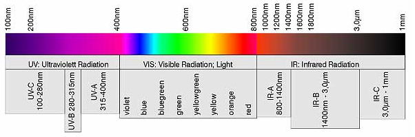
Figure 2. The solar spectrum is a subset of the EMS extending from ultraviolet (short wavelength) to infrared (long wavelength), and includes the intermediate human-visible range (courtesy Allied Vision).
Each of these three bands is further sub-categorized. Ultraviolet (UV), for example, is commonly segmented into three distinct regions, near UV (UVA, 315–400 nm), middle UV (UVB, 280–315 nm), and far UV (UVC, 180–280 nm). Visible light is similarly subdivided into separate color bands, commonly abbreviated as ROYGBIV (red/orange/yellow/green/blue/indigo/violet, ordered by decreasing wavelength i.e. increasing frequency). And infrared (IR) begins just beyond the red end of the visible light spectrum, extending from there into up to five distinct segments; near IR (NIR or IR-A, 750-1,400 nm), short wavelength IR (SWIR or IR-B, 1,400-3,000 nm), mid wavelength IR, also called intermediate-IR (MWIR or IIR, 3,000-8,000 nm), long wavelength IR (LWIR or IR-C, 8,000-15,000 nm) and far IR (FIR, 15,000-1,000,000 nm).
Infrared Imaging
Infrared imaging encompasses many different technologies, products and applications. A variety of detection devices find use depending upon the specific wavelength(s) being sensed within the infrared band. Since silicon exhibits some absorption (typically 10%-25% quantum efficiency, QE, i.e. spectral response) in the NIR range, and sunlight is comprised of nearly 50% NIR wavelengths, standard silicon-based sensors can often also be used in NIR applications. Therefore, many conventional visible-light imaging applications can be easily modified to operate in the NIR. Several methods are available to accomplish this objective. One approach, for example, leverages a standard CCD or CMOS imager, blocking visible light from reaching the sensor by adding low-pass or band-pass filters to the optics and/or imager.
Other enhancement methods involve special sensor designs, encompassing altered pixel geometry and spectrum-tailored glass/microlens arrangements, for example. For night vision implementations or when sunlight is otherwise not available, the incorporation of NIR illumination is another proven method, used extensively in security and surveillance applications. More generally, the applications for NIR imaging are numerous and growing. Biometrics has adopted NIR technology for fingerprint, vein and iris imaging, for example. Medical and forensics applications also benefit from NIR imaging, as do sports analytics, medical equipment, and machine vision. Because as previously mentioned many commercial sensors have NIR sensitivity, numerous NIR-capable cameras and camera modules are available on the market for embedded applications.
Moving from NIR to SWIR requires a transition in detector technology. Sensors used in SWIR cameras conceptually operate similar to silicon-based CCD or CMOS sensors; they convert photons into electrons, thereby acting as quantum detectors. However, in order to detect light beyond the visible spectrum, these particular detectors are comprised of materials such as indium gallium arsenide (InGaAs) or mercury cadmium telluride (MCT, HgCdTe). Although infrared radiation in the SWIR region is not visible to the human eye, it interacts with objects in a similar manner as visible wavelengths. Images from an InGaAs sensor, for example, are comparable to visible light images in resolution and detail, although SWIR images are monochrome-only.
InGaAs sensors also respond to differences in thermal energy. This makes them less sensitive to changes in light conditions, thereby rendering them effective in challenging environmental conditions such as low light, dust and haze. One major benefit of imaging in the SWIR band is the ability to image through glass. Special lenses are usually unnecessary with SWIR cameras. SWIR cameras are also used in high-temperature environments; they are ideally suited for imaging objects ranging from 250ºC to 800ºC. With respect to embedded applications, SWIR cameras do not typically meet the size, power and cost targets of most systems. Many SWIR cameras require active cooling, for example. However, ongoing design and production improvements are helping SWIR technology deliver reasonable return on investment (ROI), especially for the inspection of high-value products, for example, or in emerging medical OEM applications.
MWIR, like SWIR, requires a dedicated detector material. Mercury cadmium telluride (MCT) and indium antimonide (InSb) are most commonly used, and an integrated Dewar cooler assembly (IDCA) is also usually included in the design. MWIR camera assemblies can be complicated, but their size, weight, power and cost are steadily decreasing. They most often find use in target signature identification, surveillance, and non-destructive testing applications. They are capable of very long-range imaging, as well as detecting minute changes in temperature.
LWIR, also referred to as thermal imaging, is an approach wherein the detector responds to thermal energy rather than photons (Figure 3). Such thermal detectors operate differently than quantum (photon) detectors. Thermal detectors absorb energy, causing a localized increase in temperature, which in turn creates an electrical charge. These detectors are typically microbolometers, most commonly constructed of either amorphous silicon (a-Si) or vanadium oxide (VOx). Applications for LWIR imaging are numerous, ranging from preventive maintenance of equipment, energy audits of homes, agriculture monitoring, and border control along with other surveillance scenarios. The cost and complexity of LWIR cameras and camera cores has significantly decreased in recent years; LWIR components for consumers are even available.
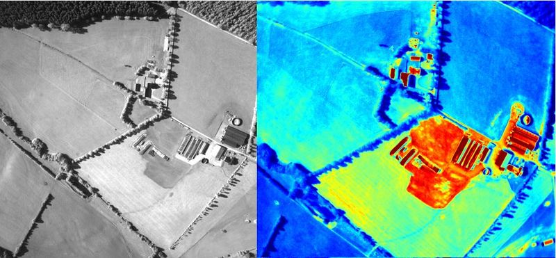
Figure 3. While a gyrocopter-mounted conventional digital machine vision camera is capable of capturing only a monochrome view of a scene (left), a LWIR camera provides additional thermal information for analysis purposes (right) (courtesy Application Center for Multimodal and Airborne Sensor Technology).
Ultraviolet Imaging
UV imaging finds use in a wide variety of applications, from industrial to medical. Two fundamental reasons for imaging with UV are the need to detect or measure very small features in an object, and to leverage the UV-sensitive properties of an object. Two main techniques for UV imaging exist: reflected imaging and fluorescence imaging. Reflected imaging combines a UV light source and a UV-sensitive detector. Since UV spans a wide range of wavelengths, wide-range UV detectors are correspondingly necessary for reflective imaging. For near UV, standard CCD/CMOS sensors deliver some relative response. However, both the sensor and optics must not include any UV filtering or coating. Sunlight may provide enough UV light for imaging in the near UV band, otherwise a secondary light source is required. For middle UV and far UV, conversely, special detectors, light sources and optics are required. These bands are relevant in some commercial imaging applications. However, as with MWIR and beyond, increased cost and design effort is required to leverage them.
Fluorescence imaging also uses a UV light source, in this case accompanied by a detector with sensitivity to another wavelength (typically somewhere in the visible band). The UV light source shines on the material(s) to be imaged, which absorbs it. The object subsequently emits photons, with the material outputting light at a longer-than-UV wavelength; blue is commonly encountered in industrial applications, for example. To effectively image the fluorescence requires the use of bandpass filters tuned for the emitted wavelength (Figure 4). Such bandpass filters block the light coming from the UV light source, which can otherwise interfere during imaging. Applications for fluorescence imaging include microscopy, and 2D data matrix recognition and inspection.
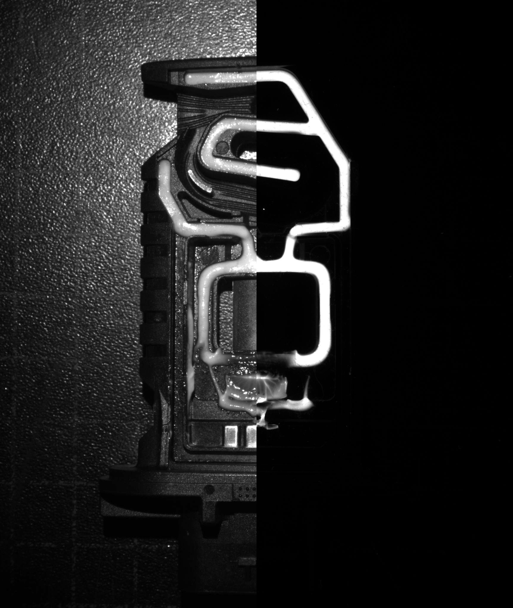
Figure 4. Normally, an object illuminated with UV light provides at best a muted fluorescence response (left). However, by filtering the UV light with a bandpass filter, the object’s photon response becomes more obvious (right) (courtesy Allied Vision).
Infrared Imaging Case Study
Use of the infrared spectrum can be beneficial for numerous real world applications. Consider agricultural applications, for example, where infrared cameras can monitor plant health in a nondestructive manner (Figure 5). LemnaTec GmbH is one company developing solutions for this particular application. LemnaTec’s Scanalyzer3D system utilizes various infrared wavelengths to monitor plant health. Agriculturalists use the information provided by Scanalyzer3D to determine reactive and proactive measures necessary to ensure robust crop growth and longevity.

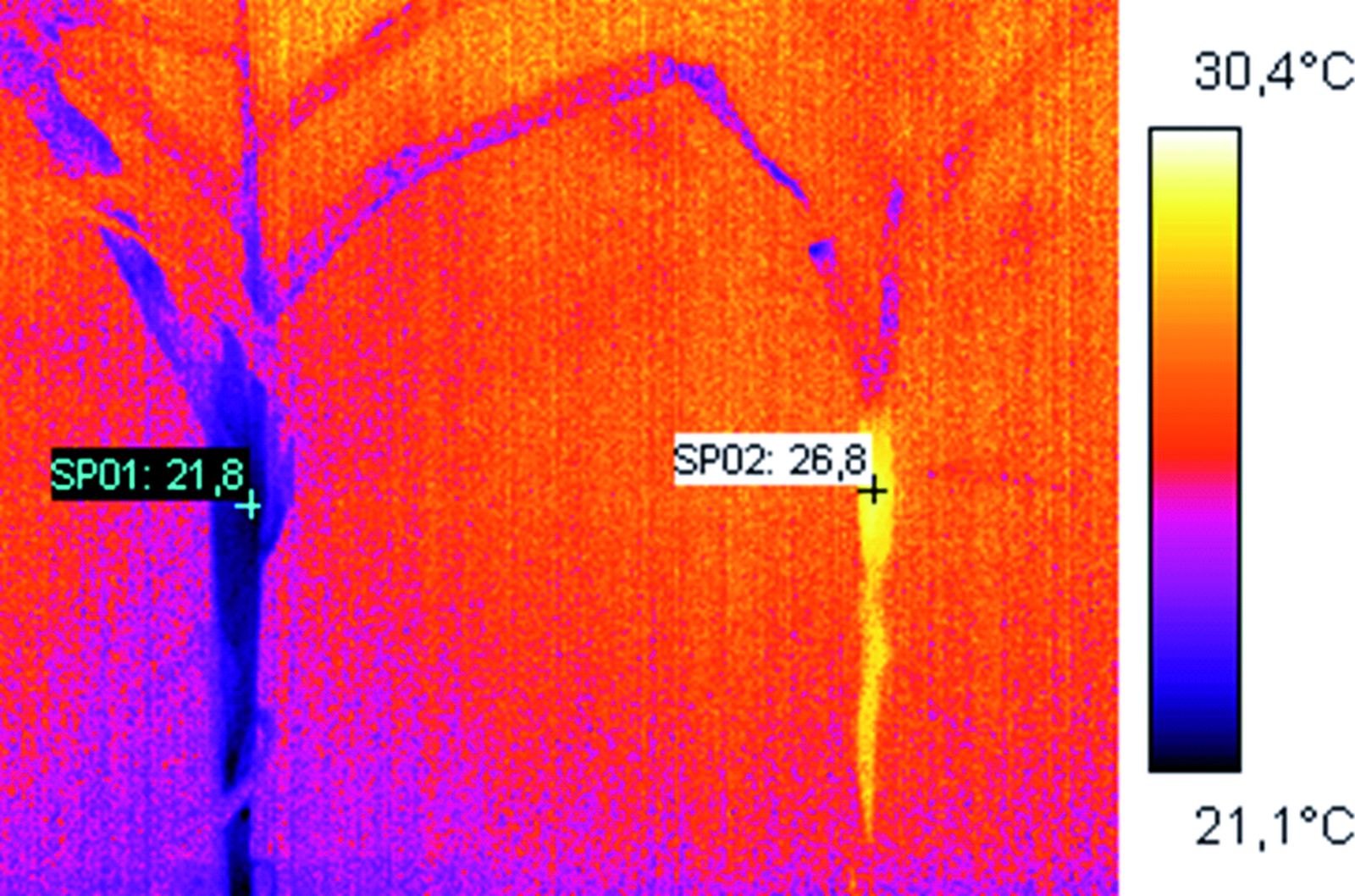
Figure 5. LemnaTec’s Scanalyzer3D IR-based imaging and analysis system enables non-destructive plant phenotyping (top). Thermal analysis, for example, generates false coloring that depicts temperature variance (bottom) (courtesy LemnaTec GmbH).
Water absorbs infrared light in the 1400 to 1500 nm wavelength range. In an infrared image, water therefore appears opaque. As a result, the areas of a plant that are darker in an infrared image reflect the presence (and relative abundance) of water in these regions. More generally, Scanalyzer3D uses multiple infrared cameras to implement the following functions:
- A LWIR camera measure the plant’s temperature, which indicates if the plant is within its ideal growing temperature range
- A NIR camera, in conjunction with a SWIR camera, detects moisture absorption in each plant, thereby determining its root system’s efficiency
- The SWIR camera also finds use in viewing each plant’s water distribution, determining if it is sufficiently hydrated
- LemnaGrid, LemnaTec’s proprietary image processing software, handles all image processing operations. It enables users to both design imaging processes and to implement various image enhancements, such as false color rendering.
Conclusion
Expanding the computer vision analysis range beyond the visual spectrum to encompass the infrared and/or ultraviolet electromagnetic spectrum, either broadly or selectively and either solely or in conjunction with visible spectrum analysis, is of great benefit in a range of visual intelligence applications (see sidebar “Multispectral and Hyperspectral Imaging”). Successfully implementing such capabilities in an embedded vision system with stringent size, weight, cost, power consumption and other constraints can be challenging. Fortunately, an industry alliance is available to help product creators optimally implement such vision processing in their resource-constrained hardware and software designs (see sidebar “Additional Developer Assistance”).
By Brian Dipert
Editor-in-Chief, Embedded Vision Alliance
Francis Obidimalor
Marketing Manager Americas, Allied Vision
Sidebar: Multispectral and Hyperspectral Imaging
Monochrome cameras, as their name implies, accept all incoming light, with no spectral differentiation. The most common cameras that selectively distinguish between different wavelengths are visible-light color cameras, in which filter arrangements such as the popular Bayer pattern are located above the surface of the image sensor(s). Only the red, green, or blue portion of the visible light spectrum passes through each filter to its associated sensor pixel. A color image is generated by these directly captured spectrum components, along with inter-pixel interpolation to create an approximation of the remainder of the visible spectrum.
In order to more precisely visualize both visible and beyond-visible light spectral signatures, a considerably larger number of selective-spectrum channels are required. Equipment that captures and analyzes fewer than 100 spectral bands is commonly known as a multispectral camera; hyperspectral cameras conversely comprehend more than 100 channels’ worth of selective-spectrum data. Conceptually common to all such spectral cameras is the splitting of incident light into many individual components, which are individually detected on different areas of the sensor surface. In contrast to conventional monochrome or color cameras, much more inbound light is needed to obtain easily evaluated images with spectral cameras.
Various technologies find use in accomplishing this fine-grained spectral splitting. For simpler situations involving comparatively few spectral bands, different band-pass filters sequentially locate in front of the sensor, in the process of capturing a long-exposure (or alternatively, multi-exposure) image. Overall spectral signature recording is accomplished via combining the data generated by this sequential individual-band recording. One perhaps obvious disadvantage of this technique is that the object being analyzed must remain completely still during the lengthy single- or multiple-exposure interval.
Today’s market is dominated by so-called “pushbroom” cameras (Figure A). This approach incorporates a narrow light gap passing through a prism or diffraction grating and subsequently projected onto an area image sensor. Since pushbroom cameras “see” only one light slot at a time, either the camera or the object being analyzed must move vertically in relation to the slot (via a drone, for example, or a conveyor belt) in order to capture area data. Pushbroom cameras are capable of achieving high spatial and spectral resolutions, up to several hundred spectral bands depending on the sensor type employed.
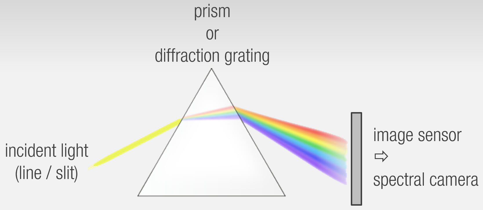
Figure A. “Pushbroom” cameras are capable of high spatial and spectral resolutions but require sequential movement of either the camera or object being visualized, with the other held completely still through the lengthy scanning interval (courtesy XIMEA).
In addition to these established approaches, emerging alternative technologies have also appeared for generating spectral differentiation at the image sensor. One approach involves the creation of fine-grained bandpass filters, conceptually similar to the previously mentioned coarse-grain Bayer color pattern, for both visible and beyond-visible light bands. Sensors developed by IMEC, a research institute in Belgium, have also recently become viable candidates for industrial use. This particular approach involves a small Fabry-Perot interference filter applied to each sensor pixel, resulting in a narrow pass-through spectral band.
Both “fan-out” filter arrangements, resembling the spectral line-scan behavior of a pushbroom camera, and “snaphot” arrangements are available. In the latter case, 4×4 or 5×5 filter patterns are constructed and replicated across the sensor surface. Advantages of the “snapshot” approach include the fact that each image captured contains a complete set of spectral information, and that the object being analyzed can be in motion. However, accompanying these advantages is a reduction in spatial resolution capability versus with other approaches.
By Jürgen Hillmann
CTO, XIMEA
Sidebar: Additional Developer Assistance
The Embedded Vision Alliance, a worldwide organization of technology developers and providers, is working to empower product creators to transform the potential of vision processing into reality. Allied Vision and XIMEA, the co-authors of this article, are members of the Embedded Vision Alliance. The Embedded Vision Alliance’s mission is to provide product creators with practical education, information and insights to help them incorporate vision capabilities into new and existing products. To execute this mission, the Embedded Vision Alliance maintains a website providing tutorial articles, videos, code downloads and a discussion forum staffed by technology experts. Registered website users can also receive the Embedded Vision Alliance’s twice-monthly email newsletter, Embedded Vision Insights, among other benefits.
The Embedded Vision Alliance also offers a free online training facility for vision-based product creators: the Embedded Vision Academy. This area of the Embedded Vision Alliance website provides in-depth technical training and other resources to help product creators integrate visual intelligence into next-generation software and systems. Course material in the Embedded Vision Academy spans a wide range of vision-related subjects, from basic vision algorithms to image pre-processing, image sensor interfaces, and software development techniques and tools such as OpenCL, OpenVX and OpenCV, along with Caffe, TensorFlow and other deep learning frameworks. Access is free to all through a simple registration process.
The Embedded Vision Alliance and its member companies periodically deliver webinars on a variety of technical topics. Access to on-demand archive webinars, along with information about upcoming live webinars, is available on the Alliance website. Also, the Embedded Vision Alliance has begun offering “Deep Learning for Computer Vision with TensorFlow,” a full-day technical training class planned for a variety of both U.S. and international locations. See the Alliance website for additional information and online registration.
The Embedded Vision Alliance’s annual technical conference and trade show, the Embedded Vision Summit, is intended for product creators interested in incorporating visual intelligence into electronic systems and software. The Embedded Vision Summit provides how-to presentations, inspiring keynote talks, demonstrations, and opportunities to interact with technical experts from Embedded Vision Alliance member companies. The Embedded Vision Summit is intended to inspire attendees’ imaginations about the potential applications for practical computer vision technology through exciting presentations and demonstrations, to offer practical know-how for attendees to help them incorporate vision capabilities into their hardware and software products, and to provide opportunities for attendees to meet and talk with leading vision technology companies and learn about their offerings.
The most recent Embedded Vision Summit took place in Santa Clara, California on May 1-3, 2017; a slide set along with both demonstration and presentation videos from the event are now in the process of being published on the Alliance website. The next Embedded Vision Summit is scheduled for May 22-24, 2018, again in Santa Clara, California; mark your calendars and plan to attend.