By Tom Catalino
Vice President
Critical Link, LLC
and
Asheesh Bhardwaj
DSP Senior Applications Engineer
Texas Instruments
This is a reprint of a Texas Instruments-published white paper, which is also available here (560 KB PDF).
Introduction
Machine vision technology is growing in adoption, and it has been and will continue to be deployed in a variety of application areas. These include instrumentation and inspection equipment used to manufacture a wide range of products as varied as sheet goods, pharmaceuticals, semiconductors, razor blades and automobiles. Each application of machine vision carries a unique set of vision system requirements that are often not readily served by preconfigured devices. This white paper addresses a particular class of machine vision systems – those that are compute intensive – by detailing an architecture and additional resources the reader can use to move forward with their own vision system design, based on this, or a similar, architecture.
Problem statement
Many machine vision system algorithms are very compute intensive and therefore may require dedicated hardware. Each application carries unique requirements that lend themselves to programmable architectures like DSP or FPGA, rather than to a dedicated, fixed-function device or core, such as vision analytics and video compression with CODEC or an ASIC.
There are a number of readily available vision products on the market today that provide the building blocks suitable for a standards-based vision system. These include open source vision algorithms from OpenCV. The standards many vision systems must support include video encoding or transcoding using a number of different standard video formats (MPEG-4, H.264, etc.) as well as a standard set of digital interfaces (USB, GigE, Camera Link, HDMI, etc.).
But what if you needed to develop a very specialized camera? Maybe you need a camera where full-resolution, high-definition video at 30 frames per second (fps) or 60 fps is not necessarily the objective. Instead, you require fully customized algorithmic processing on a small region of interest at a very high frame rate – in the thousands of fps, with 50×50 pixel resolution. At the other end of the spectrum, you might need to execute a custom algorithm on an image that is non-standard, very high resolution, at a lower frame rate with low overall power consumption. And perhaps the volumes needed for this special camera are low to medium – not enough to justify the schedule, expense or risk required for the development of a specialized ASIC.
This paper provides an architecture that addresses such unique requirements, and provides resources necessary to move forward with your own design based on the outlined concepts.
Architecture
An architecture used by Critical Link, a member of the Texas Instruments Incorporated (TI) Design Network, in a number of designs with these types of requirements leverages the Spartan-6 family of FPGAs from Xilinx, along with the power and flexibility of the TI OMAP-L138 DSP+ARM9TM processor, including use of its uPP interface. The combination of these two devices, illustrated in this paper with Critical Link’s MityDSP-L138F System on Module (SoM), allows for low-power systems that can efficiently address unique requirements.
Programmable logic with the Xilinx Spartan-6
Incorporating programmable logic into any hardware design increases the overall flexibility of the system. In this case, the Xilinx Spartan-6 is a particularly good choice as a match for the TI OMAP-L138 processor and the types of systems addressed in this paper (Figure 1). The Spartan-6 has its SelectIO, which can be configured to support a wide variety of signaling standards, including LVDS, LVTTL, LVCMOS and many others. It can be customized to interface directly to the digital imaging sensor most suitable for the system being designed. Further, it can also be used to interface to analog-based sensors, such as CCD imagers, by designing an ADC between the FPGA and the sensor itself.
Figure 1. Image processing in Xilinx FPGA
Once the image data has been acquired by the FPGA, the programmable logic can be used to quickly and efficiently perform a wide variety of operations on the data. The FPGA is well suited for operations such as edge or corner detection, extraction and low-level analytics operations. In addition, basic frame-to-frame operations can also be efficiently performed in the FPGA.
Another advantage of the FPGA is that it can be used to cull raw data down to only that data which must be touched by the DSP/applications processor. This is particularly useful when the processing requirements are more than the DSP/applications processor can handle – such as analyzing every frame of a full-resolution video stream at high frame rate, or when the sheer volume of data is higher than the processor’s digital interfaces can take in. This culling of the raw data can be performed by using the FPGA to statically or dynamically identify particular regions of the image that would be of interest to the applications processor (for example, a license plate or a face), or by using the FPGA to calculate key statistical data such as a histogram or background estimation on the images and provide this information to the OMAP-L138 processor.
The Xilinx Spartan-6 FPGA is capable of capturing the data at a very high frame rate and dropping extraneous full or partial frames. It can then pass on only the interesting data for processing in the DSP, reducing the overall bandwidth required between the FPGA and the DSP/applications processor.
Xilinx Spartan-6 devices provide up to 180 DSP48A1 slices that can be leveraged to implement high- performance video acceleration blocks using parallel hardware architecture. Xilinx also provides video- and image-processing IP cores that can be used to reduce development time.
Finally, Xilinx FPGAs are also used to implement non-standard interfaces. This could be a multiple display or multiple camera system, custom synchronous serial interfaces, a custom parallel interface, or simply added capability for additional standard interfaces for which the applications processor within the system lacks support. These interfaces can again take advantage of the variety of physical layers provided by the FPGA (LVDS, etc.).
Carrying image data from FPGA to DSP via uPP
Critical Link has used the uPP interface on the TI OMAP-L138 processor to carry image data from the Xilinx Spartan-6 to the DSP on board the OMAP-L138 processor. This interface is specifically designed to move large amounts of data continuously into or out of the processor’s memory.
The uPP can clock one data word (8 or 16 bits) per clock cycle. (Or it can handle two data words per clock for double-data-rate, but the clock speed must be half as fast.) The uPP clock rate can be up to half of the processor clock rate, with a maximum uPP clock of 75 MHz, allowing a throughput of up to 150 MBytes/s. This elegantly simple uPP interface allows for easy integration with an FPGA (Figure 2).
Figure 1. uPP Interface between the TI OMAP-L138 DSP+ARM9TM processor and an FPGA
The TI OMAP-L138 processor actually includes two uPP interfaces, each of which can be independently configured. From a hardware point of view, the uPP interface is a fairly simple synchronous data interface. It includes a clock pin, data pins and several control pins that indicate valid data and start/wait conditions. In fact, the interface can be used gluelessly with some parallel ADCs and DACs.
Using the above uPP data rates as an example, Table 1 illustrates the theoretical maximum fps that can be transferred from the Xilinx Spartan-6 FPGA to the OMAP-L138 processor system memory. Note that these calculations assume no inter-frame or inter-line gaps that may be required by the sensor. The ability of the OMAP-L138 processor’s 456-MHz ARM9TM and 456-MHz floating-point DSP to execute the intended algorithm on the data must be taken into account when sizing up a system, as this will affect the overall processed frame rate.
Table 1. Theoretical frame rates via uPP at 150 MB/s
Preferably, this should be performed through experimenting with the intended algorithms on a prototype system or evaluation module. In any case, when the application processing in the DSP or the ARM® is identified as the system design’s limiting factor, this is precisely the situation where the FPGA can be leveraged the most by identifying repetitive operations that can be moved out of the OMAP-L138 processor and into the FPGA. This leaves the DSP and ARM to attend to non-repetitive operations, more global operations, or those requiring multiple frames at once. The FPGA can be leveraged to reduce the overall data rate if the capture rate is very high and the uPP peripheral is unable to handle the full volume of raw data.
Figure 3. uPP into and out of the TI OMAP-L138 DSP+ARM9 processor
Using the uPP’s two independent channels, an architecture like that shown in Figure 3 can be conveniently implemented. Inbound data can be pre-processed by the FPGA and sent via uPP to the DSP in the OMAP-L138 processor, where it is further operated on to perform intelligent image/video analytic operations. Finally, the data can be sent back through the FPGA to any of the output interfaces. As it passes through the FPGA for the second time, low-level output processing can be performed, such as overlaying the video on top of a graphical user interface provided by the OMAP-L138’s ARM core, or providing text or other graphical overlays as directed by the DSP in the OMAP-L138 processor.
Integrated ARM and DSP processing with the OMAP-L138 processor
Up to this point, we’ve discussed data acquisition into the FPGA, FPGA processing of the data, and data transfer to the OMAP-L138 processor, a processor that provides a unique architecture for dealing with image data in and of itself – integrating a 456-MHz ARM9 applications processing core and a 456-MHz TMS320C674x DSP core (Figure 4).
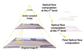
Figure 4. Image processing in the TI OMAP-L138 DSP+ARM9 processor
The combined OMAP-L138 processor + Xilinx Spartan-6 FPGA architecture is typically leveraged at Critical Link by allowing the DSP in the OMAP-L138 processor to perform the remaining algorithmic “heavy lifting” on the pre-processed image data as it arrives from the FPGA. This work can be performed by implementing custom algorithms hand-coded in C or C++ and optimized for the DSP using the TI-provided compilers in the Code Composer StudioTM integrated development environment (IDE), or by using the already optimized libraries provided by TI for image and video processing: IMGLIB and VLIB. OpenCV is an open-source library featuring many vision-related algorithms that are easy to port to the DSP.
The DSP is capable of handling computationally-intensive image analytics and processing operations, such as object detection, object identification, edge detection, color conversions, image filtering, object tracking and resizing.
Machine vision algorithms require many filtering operations for finding shapes, cracks, dirt and other anomalies on an object. Dilation, erosion, Sobel, Canny filters, Harris, Hough and Haar classifiers help with object finding and feature extraction. The object detection and tracking algorithms are mainly supported by Lucas Kanade, optical flow, Kalman filter, Bhattacharya distance and Gaussian models.
Most of the image-processing operations happen in grayscale or RGB color mode. If the captured image data is in YCbCr format, the luminance Y data can be used for grayscale processing. Depending on the type of processing needed, captured data in RGB format can either be converted to a YCbCr format or remain in the RGB format. The functions which perform extensive signal-processing algorithms are part of the either IMGLIB or VLIB, or available in OpenCV. The applications developed also utilize the DMA access to the external memory, such that the data can be transferred into internal memory for faster processing.
Moving object segmentation is an example of machine vision processing that requires video to be processed in grayscale mode with background to be deleted and foreground data to be processed. This is done with morphological operations like dilation and erosion on the foreground mask. The object boundary is formed using a connected component model (Figure 5).
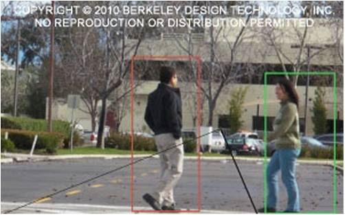
Figure 5. Moving object segmentation
Moving object segmentation with 16-bit precision has lower performance than 16-bit precision of a single Gaussian model. Depending on the type of operation needed, the approximate resolution fed to the DSP can be chosen. There will be additional 50% overhead for VLIB processing when data is in external memory (Table 2).
Table 2. VLIB performance benchmarks
External system interfaces are connected to and managed by the ARM core so that data handling and the driver’s processing load can be handled there. Careful partitioning of the computations across the three available cores will result in obtaining the most processing power out of the architecture.
As the DSP algorithmic work is being performed, the DSP can communicate with the ARM in the OMAP-L138 processor, and, through the ARM, with the external world. This may be a local or remote user interface, or may even be another processing subsystem within a larger system. The DSP may communicate with the ARM via shared memory, mailboxes or a variety of other mechanisms provided by TI’s DSPLink library. RingIO, MessageQ and Notify provide the interfaces within DSPLink for this communication. The shared memory region between the ARM and the DSP is used for sharing the data pointers between these processors. The DSPLink library increases the efficiency of data exchange.
Configuration data may be passed from the ARM to the DSP, while measurements, statistics, and raw or processed image/video data may be passed to the ARM for sharing with the outside world. The ARM is par- ticularly well suited for communications and display functions, as it can run a full-featured operating system such as Embedded LinuxTM, Windows® CE, QNX® or ThreadX.
Summary
This paper illustrates an architecture that addresses some of the widely varying requirements in the machine-vision market. This architecture leverages the power of Xilinx Spartan-6 FPGAs (though any family FPGA could be used in the design), the floating- and fixed-point DSP and ARM9TM provided in the TI OMAP-L138 processor, and the convenient and easy-to-use uPP interface peripheral that it provides.
Additional information about each of these topics can be explored through the references provided below. In particular, the MityDSP-L138F SoM and the Vision Development Kit provided by Critical Link provide a convenient platform engineers can use to further explore this architecture in their own designs.
Useful links
- Critical Link MityDSP
- Critical Link Vision Development Kit
- TI OMAP-L138 DSP+ARM9 processor
- Xilinx Spartan-6
- Xilinx image processing library
- TI IMGLIB
- TI VLIB
- TI Code Composer Studio IDE
- Open-Source OpenCV
- OpenCV on TI
References
- "An Optimized Vision Library Approach for Embedded Systems", G. Dedeoglu, B. Kisacanin, D. Moore, V. Sharma, and A. Miller, Proceedings of the IEEE Workshop on Embedded Computer Vision, pp. 8-13, 2011.
- "Moving Object Segmentation for Security and Surveillance Applications", G. Dedeoglu, D. Moore, Texas Instruments, Inc., Proceedings of the Embedded Vision Summit, September 2012.